Overview #
IN6XXE DK is a development board for IN6XXE series chips. You can download the schematics:
Hardware description #

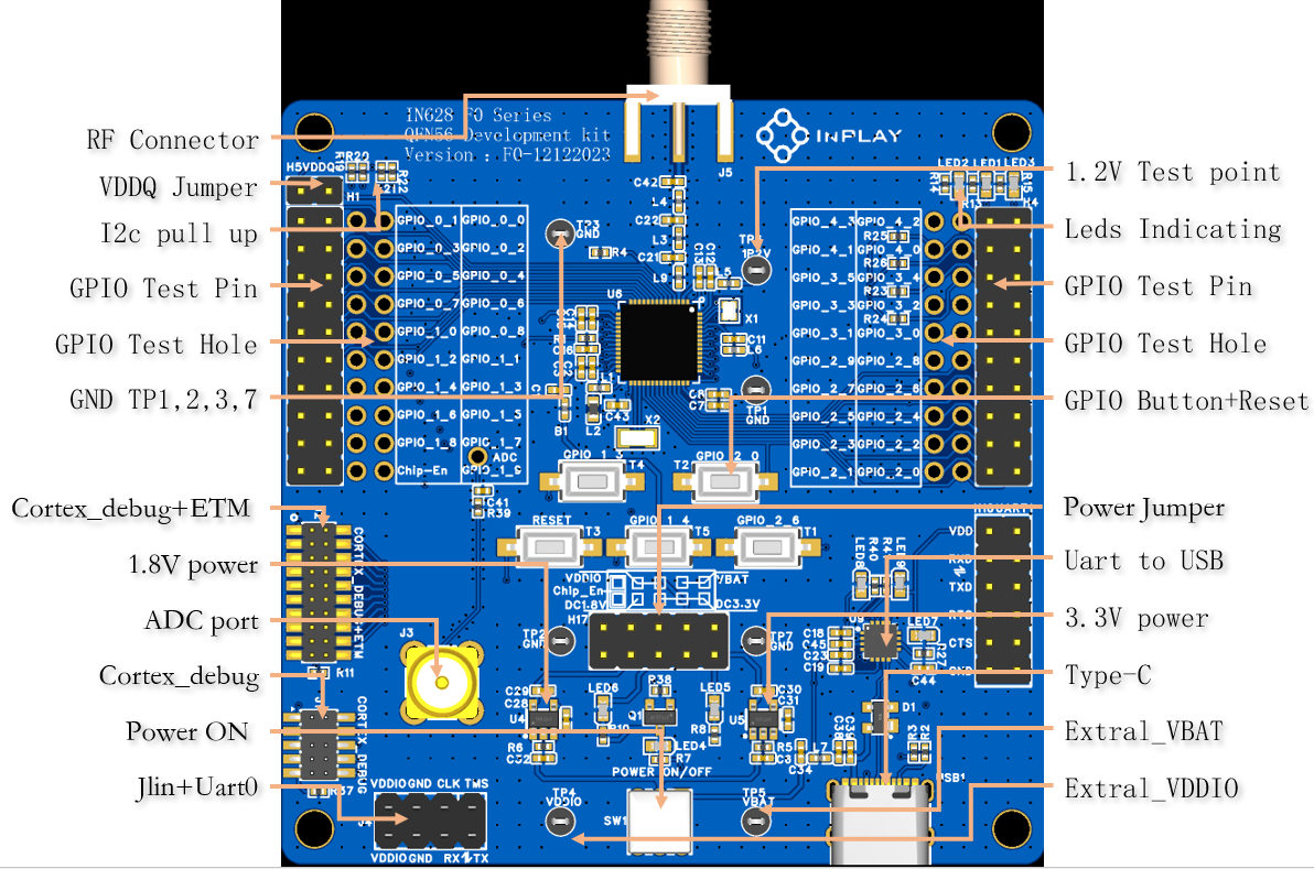
| Component | Description | |
|---|---|---|
| 1 | RF Connector | |
| 2 | I2C pull up | R19:GPIO_0_0, R20:GPIO_0_1; R21:GPIO_0_3, R22:GPIO_0_4 |
| 3 | VDDQ Jumper | When programming eFuse, connect VDDQ to 3.3V |
| 4 | GPIO Test Pin | GPIO pins |
| 5 | GPIO Test Hole | GPIO pins |
| 6 | GND TP1,2,3,7 | These test points are connected to GND |
| 7 | Power Jumper | Control power supply, see Power Supply |
| 8 | Cortex_debug+ETM | Debug port |
| 9 | 1.8V Power | 5V to 1.8V |
| 10 | ADC port | |
| 11 | Cortex_debug | Debug port |
| 12 | Power ON | Power switch of the 5V supply from USB |
| 13 | Jlink+UART0 | JLINK and UART0, UART0 Tx is GPIO_0_2, Rx is GPIO_1_0 |
| 14 | 1.2V Test point | |
| 15 | LEDs | LEDs connected to GPIO,on when GPIO drives HIGH. LED1:GPIO_2_8, LED2:GPIO_3_2, LED3:GPIO_3_3 |
| 16 | GPIO Test Pin | GPIO pins |
| 17 | GPIO Test Hole | GPIO pins |
| 18 | GPIO Button+Reset | One reset button, other buttons are LOW active(when pressed, GPIO input LOW) |
| 19 | UART Jumper | Control power supply of USB to UART chip; Control which GPIOs are connected to the USB to UART chip, default is UART1: GPIO_2_1:TX GPIO_2_7:RX GPIO_1_5:RTS GPIO_1_6:CTS see UART Configuration |
| 20 | UART to USB | USB to UART chip |
| 21 | 3.3V Power | 5V to 3.3V |
| 22 | Type-C | Power supply and connect to PC for UART port |
| 23 | External VBAT | External supply to VBAT |
| 24 | External VDDIO | External supply to VDDIO |
These components will be refered as “Component_xx”(xx is the component number) in this page.
Power Supply #
When the board is connected with USB and the switch is turned on, 5V, 3.3V and 1.8V power source will be valid, and 3 LEDs will indication the status:
- LED4: 5V
- LED5: 3.3V
- LED6: 1.8V
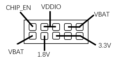
However, how these power sources will supply IN6XXE chip is configured with Power Jumper(Component_7):

CHIP_EN can always be connected to VBAT to reset the chip when powered on. VDDIO and VBAT are connected directly to the chip. VDDIO is power supply of IN6XXE’s IO, and the voltage level can be different with VBAT. These are confguration examples:
| Connections | Description |
|---|---|
| CHIP_EN<->VBAT,VDDIO<->3.3V,VBAT<->3.3V | Both VDDIO and VBAT are 3.3V, supplied with USB |
| CHIP_EN<->VBAT,VDDIO<->1.8V,VBAT<->3.3V | VDDIO is 1.8V, VBAT is 3.3V, both supplied with USB |
| CHIP_EN<->VBAT,VDDIO<->VBAT | VBAT and VDDIO are powered by external power source, can be used when measuring power consumption of the chip |
Debug Port #
There are three connectors(component 8, 11, 13) can be used as debug port, usually connected to J-Link.
UART configuration #
IN6XXE has two UART ports, UART0 and UART1. You can connect external USB to UART module to Component_13 if you use UART0.
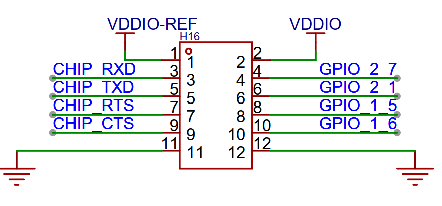
You can also use the on board USB to UART chip, configured with Component_19:

If you want to use on board USB to UART chip, 1<->2 should be connected.
If you want to use UART1(GPIO_2_1 as Tx, and GPIO_2_7 as Rx):
3<->4, 5<->6 should be connected for UART Rx and Tx.
7<->8, 9<->10 should be connected for flow control.
You can connect 4, 6 to other GPIOs if you use other GPIOs as UART port pins.
Current measurement #
If you want to measure current of IN6XXE, all pins of Component_19 should be disconnected.
For the Power Jumper, CHIP_EN<->VBAT and VDDIO<->VBAT should be connected.
Then you can connect external power source to VBAT(Component_24) and GND(Component_6) to supply power to IN6XXE and measure the current.